

A New Era in Optical Microscopy
A groundbreaking advance in optical microscopy has shattered what was once thought an unbreakable barrier — the diffraction limit. An international team of researchers has unveiled a revolutionary imaging method called ULA-SNOM, enabling scientists to see individual atoms using visible light. Until now, this level of detail was only possible with electron microscopes.
Why the Diffraction Limit Was a Problem
Traditional optical microscopes, used extensively in medicine and materials science, are limited by the diffraction of light, making it impossible to resolve structures smaller than about 200 nanometers. That meant no direct optical view of individual molecules or atoms, which are often only a few nanometers or even angstroms in size.
The ULA-SNOM Breakthrough
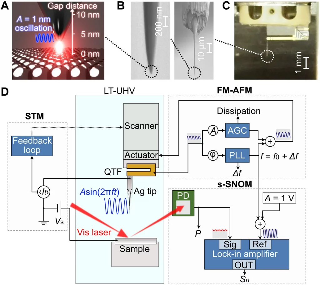
Researchers have overcome this limit with ULA-SNOM, or ultra-low amplitude scattering-type near-field optical microscopy. The technique involves scanning a sharply pointed silver tip, shaped using a focused ion beam, just 1 nanometer above the surface of a material. Illuminated by a red laser, the tip generates a plasmonic cavity — a tiny pocket of confined light — which interacts directly with atoms beneath it.
The tip’s vibrations were reduced to just 0.5–1 nanometer, small enough to avoid blurring but large enough to capture usable optical signals. This precise control enabled the device to detect genuine optical contrast between materials at the atomic scale.
Extreme Conditions for Extreme Precision
To achieve such precision, the experiment was conducted in ultra-high vacuum and at −265°C, drastically reducing noise, contamination, and mechanical vibrations. The team also used homodyne detection to suppress background light and enhance the true signal.
Real-World Results: Seeing Atom-Thick Layers
Using this technique, the researchers imaged atom-thick silicon islands on silver, distinguishing not just their physical shape, but also their optical properties. For the first time, they clearly observed how individual atoms and defects influence how a material interacts with light.
Applications Across Science and Industry
This leap in optical resolution could transform fields like nanoelectronics, quantum materials, and solar energy research. Scientists can now design materials and devices with a new level of atomic precision — paving the way for more efficient photonic components, semiconductors, and sensors.
Conclusion
The development of ULA-SNOM marks a significant step forward in nanotechnology. By pushing the limits of what optical microscopes can achieve, researchers have opened the door to atom-level visualization with visible light — a feat that could reshape the future of materials science, electronics, and beyond.


